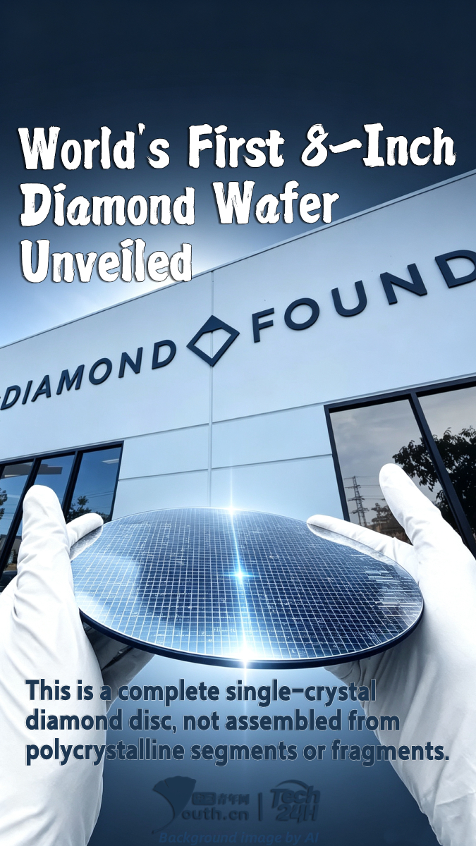
【#Tech24H】Recently, diamond semiconductor manufacturer Diamond Foundry announced it has successfully fabricated the world’s first 200 mm (8-inch) single-crystal diamond wafer (D200mm), bringing this “ultimate material” to wafer scale for the first time. This is a complete single-crystal diamond disc, not assembled from polycrystalline segments or fragments. The 200 mm diameter is roughly aligned with wafer sizes used in mature semiconductor manufacturing. It is critical to distinguish single-crystal diamond from polycrystalline diamond. Polycrystalline diamond contains grain boundaries that scatter heat carriers and electric charges; only a continuous single-crystal lattice can maximize thermal conductivity while retaining diamond’s inherent electrical insulation. This is why Diamond Foundry emphasizes that its breakthrough is a single-crystal diamond wafer. Even so, the sample wafer unveiled by Diamond Foundry is far from a qualified substrate or heat sink ready for chipmakers. Its flatness, thickness, defect density, consistency of thermal and electrical properties, and repeatability for mass production still require validation.